Dr. rer. nat. Georg Schulze-Icking-Konert
bitte mailen Sie Ihre Reprint-Anfragen, Fragen bzw.
Anregungen
an:
please mail your reprint requests, questions, or suggestions to:
Simulation and Design of an HDP-CVD Process for Planar
Spacer Applications for Future DRAM Cell Concepts
H. Weber, J. Radecker, G. Schulze-Icking-Konert, J. Bloking, W. Sabisch, A. Kersch, H. Whitesell, and Y. S. Lee
Advanced Semiconductor Manufacturing Conference (ASMC) 2006
High Density Plasma Chemical Vapor Deposition is a well known process for gap-fill applications. This paper describes the usage of High Density Plasma Chemical Vapor Deposition to generate a buried isolation layer (Planar Spacer). A study to meet Planar Spacer requirements is presented based on simulations on reactor and feature scale. It explains variations from wafer center towards the edge in within-trench fill height uniformity, sidewall coverage and hat height. Plasma density variations across the wafer surface and subsequently deviations of incoming ions off the normal direction were found as the main contributor. Simulation results could be confirmed by several experiments. Based on this results a new type of High Density Plasma Chemical Vapor Deposition process was designed to achieve homogenous within trench fill heights and pattern across the wafer and is therefore suitable for Planar Spacer applications.
Etch Rate and Profile Evolution Model for High Aspect Ratio Etch in HBr/NF3/O2 Plasma
A. Kersch, W. Jacobs, W. Sabisch, G. Schulze-Icking, A. Henke, and S. Wege
American Vacuum Society (AVS) 51st International Symposium 2004
Silicon etching based on a HBr/O2/NF3 plasma generated in a capacitively coupled Merie plasma reactor is used to fabricate DRAM trench capacitors. To maintain a constant capacitance per memory cell an optimum aspect ratio and trench shape with respect to capacitance and cost has to be achieved. In this paper we report about two feature scale models of different complexity. A compact model calculates the etch rate for a given trench geometry by solving an integral equation for the neutral and ion transport inside the trench. Input parameter are ion and fast neutral fluxes and their energy distribution as a function of CCP power, pressure, magnetic field, and the fluxes of reactive radicals as a function of plasma and gas flow conditions. The efficiency of this approach allows the investigation of effects of trench profile on the etch rate for a variety of data. A high level model calculates in addition the trench profile evolution as a function of the above parameters supplemented by the particles angular distribution, a surface scattering distribution, and a chemical rate model for etch and side wall passivation. These calculations are done with an axisymmetric/3D profile simulator (Topsi3D) which used level set front propagation, Monte Carlo particle transport, and chemical surface reaction rates. For the selection of the input parameter, a combination of experimental values (plasma density, V-I measurement, RGA) and reactor scale simulation (plasma, neutral gas flow and collisional sheath) is used. The paper focuses on the effects of power, magnetic field, pressure and gas flow on the etch rate and trench profile. The results of both models are in good agreement with each other as well as with experimental data for several technology nodes.
Top; reprint not available
Modelling CVD Effects in Atomic Layer Deposition on the Feature Scale
W. Jacobs, A. Kersch, G. Prechtl, G. Schulze Icking-Konert
International Conference on Simulation of Semiconductor Processes and Devices (SISPAD) 2004.
Simulation of atomic layer deposition requires the coupling of
complex surface chemistry to ballistic transport in geometrical
structures. The calculation furthermore has to be transient with
chemical process models which have transients on different time scales.
The paper shows a solution of this problem with a Monte Carlo based
model implemented in the general purpose feature scale simulator
Topsi3D. The chosen example is HfO2
deposition with HfCl4 / H2O
in
a
trench which may show a non-conformal film profile.
Chemical vapor deposition of tungsten silicide (WSix) for high aspect ratio applications
B. Sell, A. Sänger, G. Schulze-Icking, K. Pomplun, W.
Krautschneider
Thin Solid Films (2003) vol.443, no.1-2, p.97–107
Chemical vapor deposition of tungsten silicide into high aspect
ratio trenches has been investigated using a commercial 8-inch Applied
Materials Centura single wafer deposition tool. For an in-depth study
of both step coverage and stoichiometry, a combined
chemistry/topography simulator has been developed. Dichlorosilane
reduction of tungsten hexafluoride (WF6)
has been identified as a suitable chemistry to fill deep trenches with
tungsten disilicide, while for WF6
reduction with silane (SiH4) or disilane
(Si2H6)
fundamental drawbacks
have been identified for extreme aspect ratios. In the process range
under study, good agreement is observed between the simulated step
coverages and those obtained from scanning electron microscope
images. The simulations predict a deposition regime in which both good
step coverage and a suitable stoichiometry are achieved inside deep
trenches.
A model for Al2O3 ALD conformity and deposition rate from oxygen precursor reactivity
G. Prechtl, A. Kersch, G. Schulze Icking-Konert, W. Jacobs, T. Hecht, H. Boubekeur, U. Schröder
International Electron Devices Meeting (IEDM) 2003.
The atomic layer deposition of alumina using TMA
(Trimethyl-aluminum) and O3, O (atomic
oxygen), or H2O into high aspect ratio
trenches is investigated. We determine the activation energy of the
initial adsorption step by ab initio calculations and derive an
effective sticking coefficient. We show that this quantity essentially
determines the film conformity and deposition rate of self limiting ALD
processes. Implementing this effective model into a custom feature
scale simulator, coupled to a fluid dynamical reactor simulator, a
consistent description of ALD on atomistic, feature, and reactor scale
is obtained. With this multi scale approach it is possible for the
first time to simulate film profile evolution during dielectric ALD
into high aspect ratio trenches for future DRAM generations.
Transport Limitation Effects of Atomic Layer Deposition in High Ascept Ratio Stuctures
A. Kersch, G. Schulze Icking-Konert
European Material Research Society (E-MRS) Spring Meeting 2002
One possible cause for non-ideal ALD growth are insufficient cycle times which can result in an unsaturated surface coverage, at least at some positions of a microscopic structure. We have developed a Monte-Carlo transport simulation technique coupled to a feature scale simulator to investigate the time evolution of surface coverages during the ALD deposition step. For different precursor sticking coefficients and for structures with different aspect ratios we have calculated the minimal time required to reach complete surface saturation. Furthermore we have calculated the front of the grown film after several cycles. Our results clearly indicate that for extreme aspect ratios the cycle frequency may be limited by the gas transport inside the feature. This effect has so far been neglected but needs to be taken into account for future ALD process and equipment developments for DT processes.
Top;
not published as paper
A Feature Scale Model for Trench Capacitor Etch Rate and Profile
International Electron Devices Meeting (IEDM) 2002. Technical Digest. p.891-4
To support the optimization of aspect ratio and profile of DRAM trench capacitors we have developed two feature scale models of different complexity. A compact model calculates the etch rate for a given trench geometry by solving an integral equation for the neutral and ion transport inside the trench. This approach yields a quantitative prediction of the variation in etch rate for different trench profiles. An additional high level model calculates both the etch rate and the trench profile as a function of process parameters. This is achieved by using a level set front propagation, Monte Carlo particle transport, and chemical reaction rates. The results of both models are in good agreement with each other as well as with experimental data for several technology nodes. With our high level model it is now possible for the first time to simulate the feature evolution during deep trench etching of advanced DRAM generations.
Physically Based
Modelling of High-Density-Plasma-CVD on the Feature Scale
G. Schulze-Icking, A. Kersch, A. Knorr, A. Hausmann, J. Radecker
American Vacuum Society (AVS) 49th International Symposium 2002
Due to its low thermal budget and its highly directional deposition HDP-CVD of SiO2 has become an important process in IC fabrication. In order to study (and ultimately improve) the HDP-CVD process we have developed a physically based model for feature scale simulations. This model has been implemented into our custom Topography Simulator "Topsi" and extensive studies of the HDP-CVD process have been performed. In this presentation we give a survey of our simulation results and compare them to experiments. The model we propose retains the characteristics of a complex reactor scale model published by Meeks et al. and extends it to the feature scale. A key aspect of both models is a "structural passivation" of the surface due to the chemisorption of gas phase precursors. In contrast to conventional CVD (at much higher temperatures) in HDP-CVD this passivation is removed by cations striking the surface. Accordingly ions not only sputter surface material but also are responsible for its directional deposition. The final topography therefore is the result of simultaneous neutral deposition/passivation, ion induced activation, and sputtering. It is well known that the sputtering yield crucially depends on the ion energy and the angle of incidence. This probably also applies to ion induced surface activation, but very little is known about its energy and angular dependence. We therefore have performed deposition experiments and compared the final topography to simulations performed using our new model. With the derived set of parameters we are now able to predict the surface evolution as a function of process conditions. This is a major improvement over a more empirical model proposed by Conti et al..
Recent advances in feature scale simulation
A. Kersch, G. Schulze Icking-Konert
International Electron Devices Meeting (IEDM) 2000. Technical Digest. p.503-6
Recent developments for the simulation of kinetic energy driven processes on the submicron scale are presented. Examples include the deposition of ions (IPVD), reactive ion etching (RIE), and ion enhanced chemical reactions (new model for high density plasma deposition). The simulation results are discussed and are found to be in good qualitative agreement with experimental measurements.
Top; download;
watch void formation in test
structure
(1.3MB mpeg) and via structure (1MB mpeg)
Dissertation:
RTM-Untersuchung dynamischer
Prozesse auf Cu(111)-Oberflächen am Beispiel von
Stufenfluktuationen und epitaktisch
gewachsenen Nanostrukturen
Im Rahmen dieser Arbeit wurde der atomare Massentransport auf
Cu(111)-Oberflächen
mit Hilfe der Rastertunnelmikroskopie (RTM) untersucht. Ziel der
Studien war es,
die mikroskopischen Prozesse und Energien zu charakterisieren, welche
für die
Dynamik auf der Cu(111)-Oberfläche von Bedeutung sind.
Gleichgewichtsfluktuationen von Stufen wurden zwischen 305 K und 600 K
untersucht.
Es zeigt sich, daß unterhalb von 500 K atomare Diffusion
hauptsächlich
entlang der Stufenkanten erfolgt. Für diesen Prozess wurde eine
Obergrenze für
die Aktivierungsenergie bestimmt. Für Temperaturen oberhalb von
550 K gibt es
Hinweise auf einen Übergang zu einer dominierenden Diffusion
über die Terrasse.
Der Zerfall monoatomar hoher (bzw. tiefer) Adatom- und
Leerstelleninseln ( OstwaldReifung")
wurde zwischen 300 K und 360 K untersucht und theoretisch analysiert.
Aus dem Temperaturverhalten
des Zerfalls sowie durch numerische Rechnungen konnten die
ratenbestimmenden Diffusionsschritte
sowie relevante Energien bestimmt werden.
Bei der Untersuchung des Zerfalls mehrlagiger Inseln wurde ein
überraschendes
Verhalten beobachtet. Auf der Cu(111)-Oberfläche ist der
Interlagenmassentransport
durch eine Stufenbarriere behindert. Kommen sich zwei Stufenkanten
jedoch sehr nahe,
so verschwindet diese Barriere und ein stark überhöhter
Interlagenmassentransport
setzt ein ( Erdrutscheffekt"). Dieses Verhalten ist zur Zeit
theoretisch noch
nicht verstanden.
Top;
download (6,1MB PDF); Video
eines
atomaren Erdrutsches (Spiegelserver)
PhD Thesis: The dynamics
of
step fluctuations
and epitaxially grown nanostructures on Cu(111) surfaces as studied
using STM
This thesis deals with the investigation of atomic mass transport
on
Cu(111)-surfaces
using scanning tunneling microscopy (STM). The aim of this work was to
characterize
the relevant microscopic processes and their respective energies.
Equilibrium step fluctuations have been studied between 305 K and 600
K. The results
indicate that atomic diffusion along the step edge dominates the
dynamics of steps.
For this process an upper limit for the activation barrier has been
obtained. For
temperatures higher than 550 K, indications for a dominant diffusion
across terraces
exist.
The decay of single layer high (or deep) adatom- and vacancy islands (
"Ostwald
ripening" ) on Cu(111) has been investigated between 300 K and 360 K.
From the
temperature dependance of the decay and from numerical calculations the
the rate-limiting
processes and the relevant energies have been obtained.
The investigation of the decay of multilayer islands yielded a very
unexpected behaviour.
At steps on the Cu(111)-surface a step edge barrier slows down the
interlayer mass
transport. This barrier vanishes completely if two steps meet to form a
ledge contact.
In this case a strongly enhanced interlayer diffusion sets in (
"landslide effect"
). To date no theoretical explanation for this behaviour is available.
Top;
download
(german; 6.1MB PDF); movie
of an atomic
landslide (mirror
server)
Novel Method for the Experimental Determination of Step Energies
M. Giesen, G.Schulze Icking-Konert, H. Ibach
Physical Review Letters (1999) vol.83, no.19, p.3880-3
We describe a novel method for the determination of the absolute step energies using the temperature dependence of the equilibrium shape of adatom or vacancy islands. The method is demonstrated with islands on the Cu(111) surface.
Interlayer mass transport and quantum confinement of electronic states
G. Schulze Icking-Konert, M. Giesen, H. Ibach
Physical Review Letters (1999) vol.82, no.15, p.3101-4
A numerical analysis of the ripening of multilayer islands on Cu(111) shows that the Ehrlich-Schwoebel barrier for interlayer mass transport is independent of the terrace width w as long as w>wc=14+/-2 Angstrom, but vanishes for a terrace width below which the surface state is pushed above the Fermi level due to quantum confinement. The Ehrlich-Schwoebel barrier is therefore correlated with the occupation of surface states.
Step-step interaction energy on Cu(111) vicinal surfaces
M. Giesen, G.Schulze Icking-Konert
Surface Review and Letters (1999) vol.6, no.l, p.27-34
We have measured the terrace width distribution on copper (111) vicinal surfaces with (100) steps. For all surfaces, the distribution is well fitted by a Gaussian. The width of the Gaussian scales with the mean terrace width L, which is indicative of a repulsive L-2 interaction potential between steps. We determine an interaction strength of the potential of 3.2+/-0.2 meV per atom length. From the temperature-dependent analysis of the step-step distance distribution, we find a kink formation energy for (100) steps of 0.12+/-0.03 eV, which is consistent with previous measurements of the kink energy on copper (100) vicinal surfaces.
Fast decay of adatom islands and mounds on Cu(111): a new effective channel for interlayer mass transport
M. Giesen, G.Schulze Icking-Konert, H. Ibach
Physical Review Letters (1998) vol.80, no.3, p.552-5
We report on the observation of a new and very effective mechanism of interlayer mass transport which bypasses the Schwoebel-Ehrlich barrier for the diffusion of atoms over step edges. The channel for a rapid mass transport opens when a two-dimensional island engaged in a randam walk on a surface touches the boundary of a descending step. The decay rate of the island then increases by about 2 orders of magnitude. Even entire mounds can disappear in a very short time due to ledge contact events caused by equilibrium fluctuations of step edges.
Decay of Cu adatom islands on Cu(111)
G.Schulze Icking-Konert, M. Giesen, H. Ibach
Surface Science (1998) vol.398, no.l-2, p.37-48
We have investigated the decay of Cu adatom islands on Cu(111) as a function of temperature using scanning tunneling microscopy. By comparing the experimental results with the theory of Ostwald ripening and with numerical simulations we find that the decay is limited by the diffusion of adatoms on the terrace. From the decay rate at constant island size as a function of temperature, the sum of the energy for the formation of an adatom on the terrace and the activation energy for diffusion on the terrace is found to be 0.78+/-0.04 eV. The local environment has a significant influence on the shape of the island area versus time curves. An optimum match between simulations and experiment for the shape of the decay curves is achieved for a line tension of the islands of 0.45 eV per atom length. The Schwoebel-Ehrlich barrier for the hopping of atoms over a step is determined to be about 0.12 eV by matching the relative decay times of islands on small terraces to the simulations.
Equilibrium fluctuations and decay of step bumps on vicinal Cu(111) surfaces
M. Giesen, G.Schulze Icking-Konert
Surface Science (1998) vol.412-413, p.645-56
Using scanning tunneling microscopy we have investigated the time dependence of equilibrium step fluctuations and the time dependence of the decay of bumps in (100) steps on Cu (111) vicinal surfaces. From the analysis of the equilibrium fluctuations we find that the dominant mass transport is along the step edges with an activation energy for diffusion along a kinked step of 0.37 eV. Using this result we estimate an upper limit for the hopping barrier along (100) steps to be 0.24 eV. Nonequilibrium bumps in steps occur when wandering monatomic islands attach to a step edge. We have analyzed the time dependence of the decay of these bumps. From the Fourier representation of the bump decay we find that the dependence of the time constant on the wave number q is that of a q-4 law. This result is consistent with the analysis of the equilibrium fluctuations.
Incorporation of potassium at the Pt(111) surface
J.B. Hannon, M. Giesen, C. Klünker, G.Schulze Icking-Konert, D. Stapel, H. Ibach, J.E. Müller
Physical Review Letters (1997) vol.78, no.6, p.1094-7
Using electron-energy-loss spectroscopy and scanning tunneling microscopy, we find that at room temperature the binding site of K at the Pt(111) surface changes with increasing coverage. At low coverages, K adsorbs at surface hollow sites, forming an ionic bond with the substrate. Above a coverage of 0.1 monolayers, we observe a slow migration of K to subsurface binding sites in the second Pt layer. The measured vibrational frequencies are in quantitative agreement with cluster calculations for the proposed surface and subsurface bonding geometries.
Step fluctuations on Pt(111) surfaces
M. Giesen, G.Schulze Icking-Konert, D. Stapel, H. Ibach
Surface Science (1996) vol.366, no.2, p.229-38
We have investigated the temperature dependence of equilibrium fluctuations of monatomic steps on Pt(111) surfaces using space and time correlation functions. From the spatial correlation function of steps we have determined a kink energy of 0.167+/-0.005 eV for steps with (100) orientation. The same value was found for steps with (111) orientation. The time dependence of the correlation function obeys a t1/4 power law, provided that the mean square of the fluctuations is in the macroscopic limit. The t1/4 power law is indicative of mass transport along the steps. >From the temperature dependence of the time fluctuations an activation energy of 1.0+/-0.16 eV is determined for the hopping of atoms along steps of either orientation.
Diplomarbeit: Die
chemische
Bindung von
CO an kleinen Pt-Partikeln
In der vorliegenden Arbeit werden Photoelektronenspektren an
negativ
geladenen Clustern
(PES(A)) von PtnCOm mit den Photonenenergien
4,025 eV und 2,897
eV vorgestellt. Diese Methode erlaubt die Untersuchung des Valenzbandes
massenseparierter
Cluster in der Gasphase. Die erreichte Energieauflösung von 15 meV
ermöglicht
die Beobachtung von Vibrationsanregungen durch den
Detachmentprozeß von Elektronen.
Durch gepulste Zugabe von CO ist es möglich, mit der benutzten
Apparatur neben
den reinen und gesättigten Clustern auch Zwischenprodukte zu
erzeugen und zu
spektroskopieren. Damit stellen diese Untersuchungen meines Wissens die
ersten PES(A)-Messungen
an ungesättigten Pt-Cluster Anionen dar. Sie erlauben, die
Entwicklung der elektronischen
Struktur vom reinen bis zum gesättigten Cluster zu verfolgen.
Master Thesis: The
chemical
binding of
CO to small Pt particles
In this work photoelectron spectra of negatively charged PtnCOm
clusters (PES(A)) are presented which were obtained at photon energies
of 4.025 eV
and 2.897 eV. This method allows the examination of the valence band of
mass separated
clusters in the gas phase. The achieved energy resolution of 15 meV
enables us to
study vibrational excitations due to electron detachment.
Adding pulses of CO to the cluster beam we have been able to study
bare, saturated
and intermediate PtnCOm clusters. To my best
knowledge these
measurements represent the first PES(A) measurements of unsaturated Ptn
anions. This technique allows us to study the evolution of the
electronic structure
from bare to saturated clusters.
Top; download (german; 2MB PDF)
Bonding of CO to metal particles: photoelectron spectra of Nin(CO)-m and Ptn(CO)-m clusters
G. Schulze Icking-Konert, H. Handschuh, G. Ganteför, W. Eberhardt
Physical Review Letters (1996) vol.76, no.7, p.l047-50
Photoelectron spectra of mass-selected negatively charged bare Ni-n and Pt-n clusters are compared with the spectra of Nin(CO)-m and Ptn(CO)-m clusters. The spectra indicate that saturation with CO is caused by the formation of an electronic closed shell and not due to steric hindrance as on a surface, and that the strength of the p backdonation of the CO chemisorption bond to a small particle is stronger than to a surface. The antibonding metal dz2 -5s orbital resulting from the interaction of the CO 5s with the metal dz2 orbitals is directly observed for Ni1(CO)-3.
CO chemisorption on Nin, Pdn and Ptn clusters
G. Ganteför, G. Schulze Icking-Konert, H. Handschuh, W. Eberhardt
International Journal of Mass Spectrometry and Ion Processes (1996) vol.159, p.81-109
Vibrationally resolved photoelectron spectra of mass-selected negatively charged Ni-n=1-3, Pd-n=2,3 and Pt-n=1-4 clusters are compared with the corresponding spectra of these clusters ligated with m CO molecules (m=1-8). The spectra of the Ptn(CO)-m species reveal part of the valence orbitals, which actually form the chemisorption bond. The data are in good agreement with the Blyholder model for CO chemisorption (s-donation p-backdonation scheme) and indicate that saturation corresponds to the formation of a closed electronic shell of the neutral. The strength of the p-backdonation is found to be larger for small particles compared with the corresponding single crystal surfaces, which may be related to the catalytic properties of small particles. The spectra of the unsaturated Nin(CO)-m show fundamental differences compared with the ones of Ptn(CO)-m clusters owing to the high degree of localization of the Ni 3d orbitals. The spectra of the Pdn(CO)-m species show a rather irregular behaviour.
Thermionic emission from small clusters: direct observation of the kinetic energy distribution of the electrons
H. Weidele, D. Kreisle, E. Recknagel, G.Schulze Icking-Konert, H. Handschuh, G. Ganteför, W. Eberhardt
Chemical Physics Letters (1995) vol.237, no.5-6, p.425-31
Photoelectron spectra of small mass-separated W-n clusters cooled in a seeding gas are recorded with a low laser flux that ensures single-photon events. The spectra exhibit (i) sharp features due to direct photoemission and (ii) a broad emission signal whose intensity decreases with increasing kinetic energy. The latter is caused by delayed electron emission, a process similar to bulk 'thermionic emission'. The kinetic energy distribution of these electrons can be approximated by a Boltzmann function with a temperature corresponding to the photon energy divided by the number of vibrational degrees of freedom of the cluster.
Electronic and geometric structure of small mass selected clusters
G. Ganteför, C.Y. Cha, H. Handschuh, G.Schulze Icking-Konert, B. Kessler, O. Gunnarsson, W. Eberhardt
Journal of Electron Spectroscopy and Related Phenomena (1995) vol.76, p.37-45
An experimental setup for photoelectron spectroscopy on mass selected cluster anions is described. The photoelectron spectra reveal the electronic structure of the particles as function of their size (mass). For clusters consisting of elements which are counted among the simple metals, i.e., the alkalis as well as Cu, Ag, and Au, the electronic structure is indicative of extended, delocalized states formed by the atomic s-electrons. This is the first indication of metallic behaviour even though the particles containing up to 20 atoms clearly exhibit a 'bandgap' in the electronic structure. Additionally, in cases where vibrational fine structure is observed in the photoelectron spectra, the measured vibrational quanta allow to deduce the particle geometry. This is especially helpful in studies of chemisorption phenomena on the clusters. Moreover, electron phonon coupling constants can be extracted from a high resolution spectrum of C-60, which confirm the alkali doped fullerenes to be conventional BCS type superconductors.
Vortrag über einen einfachen Bytecode-Interpreter für kleine μControllern bis zu PCs, am Beispiel des muBoards welches bei Bosch zum Testen von Schaltungen benutzt wird.
Presentation about a simple bytecode interpreter compatible from small μCs to PCs.
Shown example is the muBoard used at Bosch for circuit testing.
Übersichtsvortrag zur Kfz-Elektronik, konkret Trend zur Embedded-Control, verteilte Intelligenz und Vernetzung.
Introductory presentation on automotive electronics. Mainly trend
towards embedded control, distributed intelligence, and networking.
Übersichtsvortrag zur physikalischen Simulation in der
Halbleiterindustrie. Schwerpunkt auf Skaleneffekte und Mixed-Scale
Simulationen
Introductory presentation on physical simulationin the semiconductor
industry. Focus on scale effects and mixed scale simulations
Simulationsvortrag zur Plasma-CVD von SiO2. Schwerpunkt
ballistischer Gasphasentransport und Oberflächenchemie
presentation on modelling of plasma-CVD of SiO2. Focus on ballistic
gas transport and surface kinetics
Simulationsvortrag zur Deep-Trench Plasmaätzung für DRAM
Speicherzellen. Schwerpunkt 1D-Gasphasentransport und Plasmachemie
presentation on modelling of deep trench etch for DRAM capacitors.
Focus on 1D Kundsen transport and plasma kinetics
Vortrag über physikalische Simulation in der IC-Herstellung. Schwerpunkt auf Reaktorsimulation und Reaktionskinetic
Presentation on physical simulation of semiconductor processing.
Emphasis on reactor-scale simulations and reaction kinetics
 |
Gasphasenabscheidung
mit
einem
Haftkoeffizienten von s=0,05 in eine Leitung mit einem
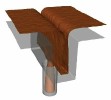
darunterliegenden Via. Deutlich ist eine Hohlraumbildung zu erkennen Gas phase deposition with a sticking coefficient of s=0.05 into a line with a via underneath. The resulting void is clearly visible |
 |
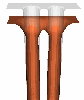
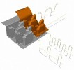
Gasphasenabscheidung
mit
einem
Haftkoeffizienten von s=0,2 in eine 3D-Teststruktur. Die
lokale Depositionsrate ist farbkodiert Gas phase deposition with a sticking coefficient of s=0.2 into a 3D test structure. The local deposition rate is color-coded |
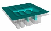 |
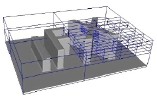
Ideal
konforme Gasphasenabscheidung in eine 3D-Teststruktur ideally conform gas phase deposition into a 3D test structure |
 |
DRAM
Deep-Trench Plasmaätzung mit Zusetzen durch unzureichende
Ätzkomponente plasma etch of DRAM deep trench capacitor exhibits clogging due to insufficient etching |
 |
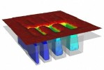
Ideale
Plasma-Gasphasenabscheidung (HDP-CVD) in eine 3D-Teststruktur. Die sich
ergebende , lokal deutlich unterschiedliche Filmdicke ist deutlich zu
erkennen, selbst unter idealisierten Bedingungen Ideal plasma gas phase deposition (HDP-CVD) into a 3D test structur. The resulting film thickness varies significantly, even under these idealized conditions |
 |
Aufbau des
Octrees zur Beschleunigung der Transportberechung mittels Monte-Carlo
Raytracing Construction of the octree for acceleration of the flux calculation via Monte-Carlo raytracing |
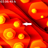 |
Zerfall
einer 3D homoepitaktischen Cu-Insel auf Cu(111), aufgenommen mittels RTM, im Rahmen meiner Dissertation decay of a 3D homoepitactical Cu island on Cu(111), measured via STM during my PhD-thesis |